- 您现在的位置:买卖IC网 > Sheet目录489 > NTHD3102CT1G (ON Semiconductor)MOSFET N/P-CH COMPL 20V CHIPFET
�� �
�
�NTHD3102C�
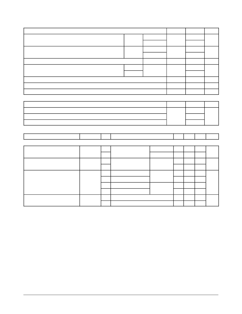
�MAXIMUM� RATINGS� (continued)� (T� J� =� 25� °� C� unless� otherwise� noted)�
�Parameter�
�Symbol�
�Value�
�Unit�
�N?Channel�
�Continuous� Drain� Current� (Note� 3)�
�P?Channel�
�Continuous� Drain� Current� (Note� 3)�
�Power� Dissipation� (Note� 3)�
�Pulsed� Drain� Current�
�Steady�
�State�
�Steady�
�State�
�N?Ch�
�T� A� =� 25� °� C�
�T� A� =� 85� °� C�
�T� A� =� 25� °� C�
�T� A� =� 85� °� C�
�T� A� =� 25� °� C�
�tp� =� 10� m� s�
�I� D�
�I� D�
�P� D�
�I� DM�
�3.0�
�2.2�
�2.3�
�1.7�
�0.6�
�16�
�A�
�A�
�W�
�A�
�P?Ch�
�12.6�
�Operating� Junction� and� Storage� Temperature�
�Source� Current� (Body� Diode)�
�Lead� Temperature� for� Soldering� Purposes� (1/8� ″� from� case� for� 10� seconds)�
�T� J� ,� T� STG�
�I� S�
�T� L�
�?55� to� 150�
�1.7�
�260�
�°� C�
�A�
�°� C�
�THERMAL� RESISTANCE� RATINGS�
�Parameter�
�Junction?to?Ambient� ?� Steady� State� (Note� 2)�
�Junction?to?Ambient� ?� t� ≤� 5� s� (Note� 2)�
�Junction?to?Ambient� ?� Steady� State� (Note� 3)�
�Symbol�
�R� q� JA�
�Max�
�110�
�60�
�195�
�Unit�
�°� C/W�
�ELECTRICAL� CHARACTERISTICS� (T� J� =� 25� °� C� unless� otherwise� noted)�
�Parameter�
�Symbol�
�N/P�
�Test� Conditions�
�Min�
�Typ�
�Max�
�Unit�
�OFF� CHARACTERISTICS�
�Drain?to?Source� Breakdown� Voltage�
�(Note� 4)�
�Drain?to?Source� Breakdown� Voltage�
�V� (BR)DSS�
�V� (BR)DSS� /T� J�
�N�
�P�
�N�
�V� GS� =� 0� V�
�I� D� =� 250� m� A�
�I� D� =� ?250� m� A�
�20�
�?20�
�20.2�
�V�
�mV/� °� C�
�Temperature� Coefficient�
�P�
�16.2�
�Zero� Gate� Voltage� Drain� Current�
�I� DSS�
�N�
�P�
�V� GS� =� 0� V,� V� DS� =� 16� V�
�V� GS� =� 0� V,� V� DS� =� ?16� V�
�T� J� =� 25� °� C�
�1.0�
�?1.0�
�m� A�
�N�
�P�
�V� GS� =� 0� V,� V� DS� =� 16� V�
�V� GS� =� 0� V,� V� DS� =� ?16� V�
�T� J� =� 85� °� C�
�5.0�
�?5.0�
�Gate?to?Source� Leakage� Current�
�I� GSS�
�N�
�V� DS� =� 0� V,� V� GS� =� ±� 8.0� V�
�±� 100�
�nA�
�P�
�V� DS� =� 0� V,� V� GS� =� ±� 8.0� V�
�±� 100�
�Stresses� exceeding� Maximum� Ratings� may� damage� the� device.� Maximum� Ratings� are� stress� ratings� only.� Functional� operation� above� the�
�Recommended� Operating� Conditions� is� not� implied.� Extended� exposure� to� stresses� above� the� Recommended� Operating� Conditions� may� affect�
�device� reliability.�
�2.� Surface?mounted� on� FR4� board� using� 1� in� sq� pad� size� (Cu� area� =� 1.127� in� sq� [1� oz]� including� traces).�
�3.� Surface?mounted� on� FR4� board� using� the� minimum� recommended� pad� size� (Cu� area� =� TBD� in� sq).�
�4.� Switching� characteristics� are� independent� of� operating� junction� temperatures.�
�http://onsemi.com�
�2�
�发布紧急采购,3分钟左右您将得到回复。
相关PDF资料
NTHD3133PFT3G
MOSFET P-CH SGL 20V CHIPFET
NTHD4102PT3G
MOSFET P-CH DUAL 20V CHIPFET
NTHD4401PT3G
MOSFET 2P-CH 20V 2.1A CHIPFET
NTHD4502NT1
MOSFET N-CHAN DUAL 30V CHIPFET
NTHD4508NT1G
MOSFET 2N-CH 20V 3.1A CHIPFET
NTHD4N02FT1G
MOSFET N-CH 20V 2.9A CHIPFET
NTHD4P02FT1G
MOSFET P-CH 20V 2.2A CHIPFET
NTHD5903T1G
MOSFET PWR P-CH DUAL20V CHIPFET
相关代理商/技术参数
NTHD3133PF
制造商:ONSEMI 制造商全称:ON Semiconductor 功能描述:Power MOSFET and Schottky Diode -20 V, FETKY, P-Channel, -4.4 A, with 3.7 A Schottky Barrier Diode, ChipFET?
NTHD3133PFT1G
功能描述:MOSFET PFET FETKY 20V CHIPFET RoHS:否 制造商:STMicroelectronics 晶体管极性:N-Channel 汲极/源极击穿电压:650 V 闸/源击穿电压:25 V 漏极连续电流:130 A 电阻汲极/源极 RDS(导通):0.014 Ohms 配置:Single 最大工作温度: 安装风格:Through Hole 封装 / 箱体:Max247 封装:Tube
NTHD3133PFT3G
功能描述:MOSFET -20V -4.4A P-CHANNEL W/3.7A SCHOTTKY RoHS:否 制造商:STMicroelectronics 晶体管极性:N-Channel 汲极/源极击穿电压:650 V 闸/源击穿电压:25 V 漏极连续电流:130 A 电阻汲极/源极 RDS(导通):0.014 Ohms 配置:Single 最大工作温度: 安装风格:Through Hole 封装 / 箱体:Max247 封装:Tube
NTHD4102P
制造商:ONSEMI 制造商全称:ON Semiconductor 功能描述:Power MOSFET -20 V, -4.1 A, Dual P-Channel ChipFET
NTHD4102P_05
制造商:ONSEMI 制造商全称:ON Semiconductor 功能描述:Power MOSFET -20 V, -4.1 A, Dual P-Channel ChipFET
NTHD4102PT1
功能描述:MOSFET -20V -4.1A Dual RoHS:否 制造商:STMicroelectronics 晶体管极性:N-Channel 汲极/源极击穿电压:650 V 闸/源击穿电压:25 V 漏极连续电流:130 A 电阻汲极/源极 RDS(导通):0.014 Ohms 配置:Single 最大工作温度: 安装风格:Through Hole 封装 / 箱体:Max247 封装:Tube
NTHD4102PT1G
功能描述:MOSFET -20V -4.1A Dual P-Channel RoHS:否 制造商:STMicroelectronics 晶体管极性:N-Channel 汲极/源极击穿电压:650 V 闸/源击穿电压:25 V 漏极连续电流:130 A 电阻汲极/源极 RDS(导通):0.014 Ohms 配置:Single 最大工作温度: 安装风格:Through Hole 封装 / 箱体:Max247 封装:Tube
NTHD4102PT3G
功能描述:MOSFET PFET 20V 4.8A 80M RoHS:否 制造商:STMicroelectronics 晶体管极性:N-Channel 汲极/源极击穿电压:650 V 闸/源击穿电压:25 V 漏极连续电流:130 A 电阻汲极/源极 RDS(导通):0.014 Ohms 配置:Single 最大工作温度: 安装风格:Through Hole 封装 / 箱体:Max247 封装:Tube